Samsung and TSMC Commit to ASML's High-NA EUV Tools
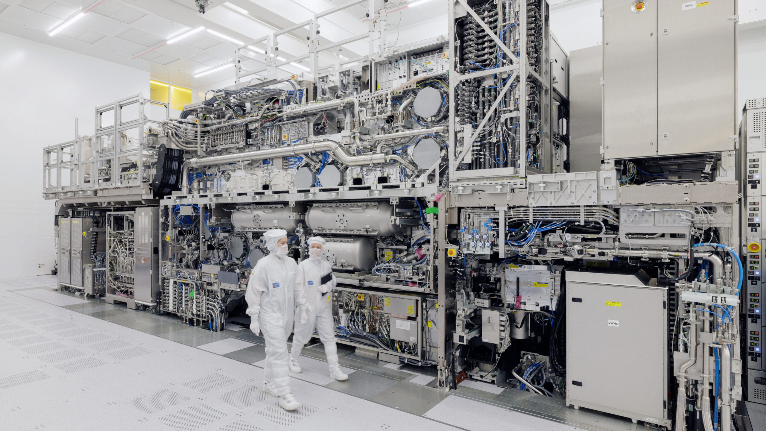
Samsung and TSMC Commit to ASML’s High-NA EUV Tools
Samsung Electronics and TSMC have both committed to adopting ASML’s newest High-NA EUV photolithography tools, multi-hundred-million-dollar machines that will be deployed over the coming years for next-generation chips. Human coverage notes that these tools, alongside Intel’s adoption, will rely on a transition to larger 12-inch photomasks, a shift expected to boost productivity by roughly 40 percent and to help print smaller circuit patterns required for advanced DRAM and logic devices.
Across sources, the shared context is that ASML is the sole provider of EUV lithography systems and that adoption of High-NA EUV is seen as a crucial enabler for future process nodes as traditional scaling becomes harder. Reports consistently tie this move to surging demand from AI data centers and increasingly complex consumer electronics, framing the investments as part of a broader industry effort to maintain Moore’s Law–style progress, secure long-term capacity, and support more computationally intensive workloads.
Areas of disagreement
Strategic framing. AI-aligned accounts typically portray Samsung and TSMC’s commitments as an almost inevitable technological step in a linear roadmap toward smaller nodes, while Human outlets emphasize it as a strategic business decision shaped by competition among the top three chipmakers and customer demand signals. AI coverage tends to present the High-NA shift as a neutral infrastructure upgrade, whereas Human coverage underlines how this consolidates ASML’s leverage and may lock in long-term supplier–foundry dependencies. Human reporting also places more weight on how these commitments affect competitive positioning against rivals like Intel.
Economic implications. AI sources often focus on the technical benefits and mention cost only in passing, framing the $400 million-class tools as necessary capital expenditures for continued scaling. Human coverage more explicitly discusses the economic stakes, highlighting how the 40 percent productivity gain from 12-inch masks is needed to offset tool cost and improve fab economics. While AI narratives lean toward the inevitability of spending for performance gains, Human reports stress return on investment, pricing power, and how these bets relate to AI-driven demand cycles and potential overcapacity risks.
Industry risks and constraints. AI-aligned reporting generally downplays or abstracts away execution risks, implying that once committed, deployment of High-NA EUV will proceed smoothly within existing roadmaps. Human coverage flags more constraints, such as ASML’s production bottlenecks, integration challenges of High-NA tools into fabs, and the possibility that schedule slips or yield issues could ripple through DRAM and logic roadmaps. Human outlets also more often invoke geopolitical and export-control context, whereas AI narratives usually treat the development as a largely apolitical technology story.
Impact on innovation. AI sources tend to frame High-NA EUV as a universal accelerator of innovation that will naturally support more advanced AI workloads and consumer products. Human coverage more carefully differentiates which segments benefit most, noting that next-generation DRAM and cutting-edge AI accelerators gain disproportionately while mature-node products may see little effect. Human articles also question whether reliance on a single lithography vendor could slow or concentrate innovation, a nuance that AI accounts are less likely to explore.
In summary, AI coverage tends to present Samsung and TSMC’s High-NA EUV commitments as a mostly technical, linear progression in chip scaling, while Human coverage tends to foreground strategic, economic, and risk-oriented nuances around ASML’s role, capital intensity, and the industry-wide consequences of these decisions.
Continue reading https://foxvector.com/stories/01a08555-c135-2beb-7080-1df52c094526
Write a comment